Objective:The objective of this activity was to create something that would detect a paper jam. When there is a paper jam, a light and buzzer should go off. There are three switches, when paper is present the switch will output a logic of 1, when there isn't paper present it will output a logic of 0. When two adjacent switches are pressed, there is a paper jam present. Once the paper is removed the light should go off but the buzzer should not until a reset button is pressed.
|
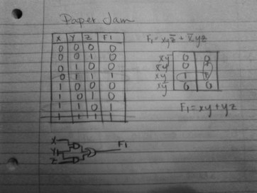
Brainstorming:To start off, i created a truth table to find the equation that would represent all possible combinations that would set off the paper jam light and buzzer. After finding the equation from the original truth table, i then used K-Mapping to simplify the equation. For an explanation of K-Mapping click on the button below.
After finding the simplified logic expression, i then figured out what logic i would need to use. In this case is used two AND gates and a NOR gate. The picture to the left is the logic equation and image of the logic i used. |
Parts List:
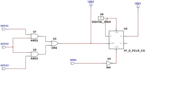
Next, i asked myself, what will i need to design and create this paper jam detector? To start out i knew i would need 3 switches, when using a DLB, the switches are know as GPIO's. Below in the Multi-Sim design you will see these on the very left hand side.
After that I looked back at the logic i had drawn up in my brainstorming process and knew that 2 NAND gates and one OR gate would be required to put together all the possible inputs to one output of 1 (which means the light and buzzer will go off).
In the objective it is said that the buzzer must not go off until a reset button is pushed. In order to do it would have to be ran through a flip flop, in this activity a D and Q flip flop is used (ff_D_PCLR_CO). An inverter is also needed, so that when the button is pressed, instead of producing a logic 1 it will produce a logic 0 therefor resetting the entire thing.
Lastly a power source is need, which is the Digital High, and two LED's are needed. One represents the light that goes off and the other represents the buzzer.
LIST:
-GPIO pins (1-3)
- 2 NAND gates
- 1 OR gate
- 1 Inverter
- FF_D_PCLR_CO (Flip flop)
- A Digital High (Power source)
- BTN1 (Reset button)
-2 LED lights.
Multi-Sim Design: