3.2.2-3.2.3 Objective:
1) Create a 3 Bit Mod 6 UP counter with 74LS74 D flip-flops in a Circuit Design Software (MUltisim) 2) Then build it on a Digital Logic Board, to see if it works as expected. 3) After confirming that it works on the Digital Logic Board, recreate the circuit in a PLD format 4) Download and test the circuit on a Digital Logic Board, using the field programmable gate array.
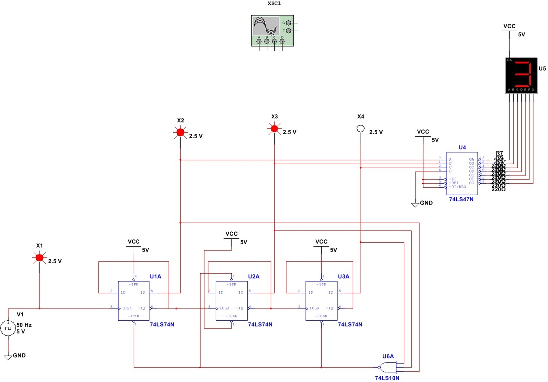
Step 1: Build 3-Bit Mod 6 Up Counter in Multi-Sim
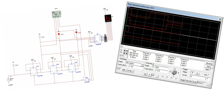
I started off my entering the provided circuit into multi-sim, then i attached a four channel oscilloscope to monitor the signals. Below to the left is a picture of the circuit entered into multi-sim. Below to the right, is the oscilloscope when it changes from the count 5-0. (Click to enlarge).
|
After creating the 0-5 Counter, we then had to modify the circuit to count from 2-6. To the right is the modified circuit. To get the counter to reset at seven, you first had to wire all of the inputs of the NAND gate to Q, then you had to wire the preset of the second flip flop to reset, and then wiring the clear to 5V.
|

|
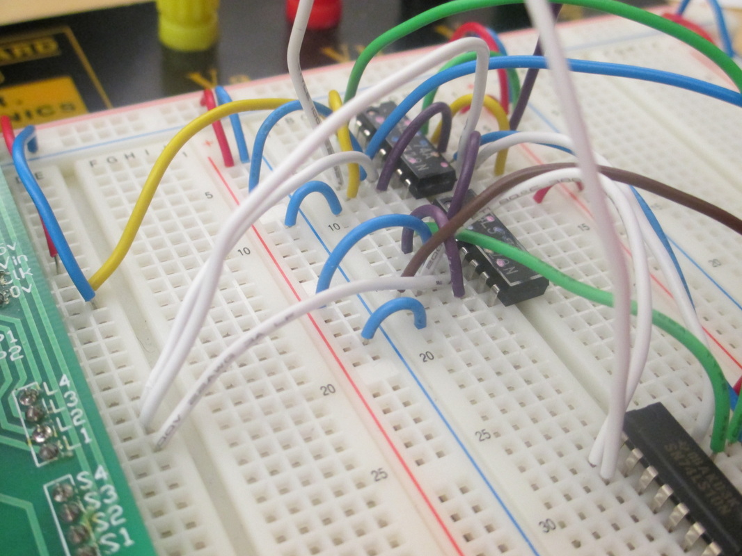
Step 2: Build and Test the 0-5 Counter and the 2-6 Counter on a Breadboard (Digital Logic Board).
To build the circuit on a bread board, the D flip flop gates, a NAND gate, Resistors, and a Seven Segment display were needed. I built the circuit following the multi- sim drawing. Below to the left is the D-Flip Flops (74LS74N), using a data sheet and the multi-sim circuit, i wired the appropriate wires to the designated places.
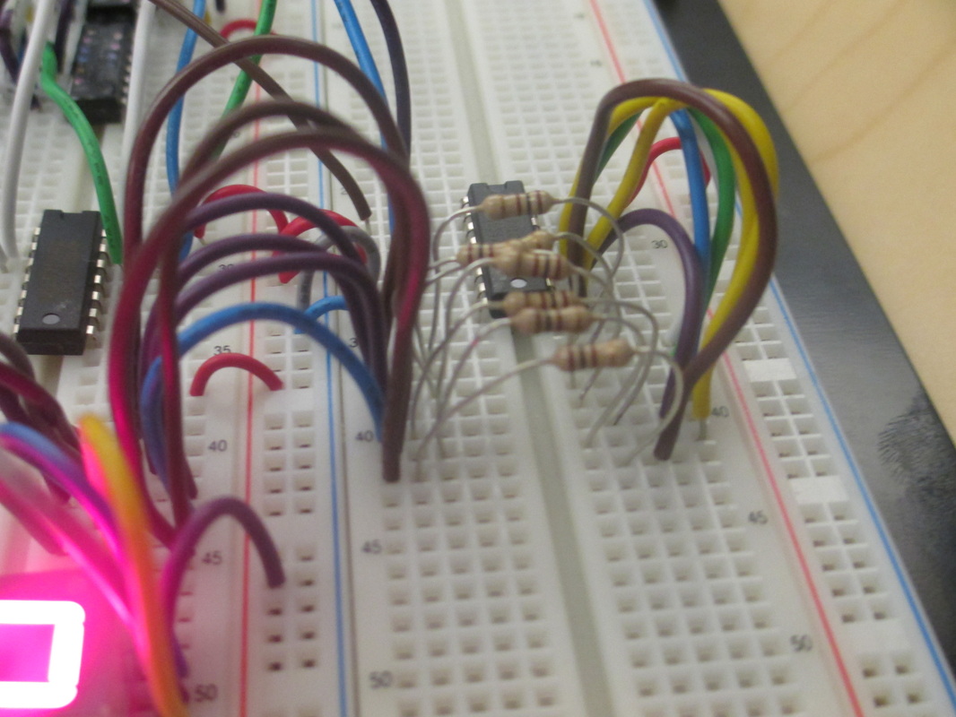
To the right is the NAND gate, with the required amount of resistance used to wire it to the Seven Segment Display.
To the right is the NAND gate, with the required amount of resistance used to wire it to the Seven Segment Display.
|
|
0-5 Counter |
0-6 Counter |
Step 3: Re-Implement 3 Bit MOD counter in a FPGA (Field Programmable Gate Array)
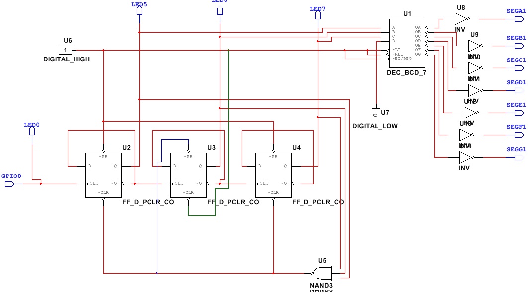
To re create this circuit, i started out by redesigning the circuit in a PLD form, because some of the things that were available in the first implementation are not in this one, for example the D flip flop (74LS74N) has to be replaced with FF_D_PCLR_CO, it does the same thing as a D flip flop. There are a few other things that had to be replaced. Below is a picture of the FPGA circuit design, compared to the original on the right hand side.
|
|
To build the circuit on the DLB board using FPGA, you simply download the circuit onto the board and wired up the Roc Clock, which is used in place of the other clock on the first bread boarding exercise.
0-5 FPGA Counter |
2-6 FPGA Counter |
Conclusion
Implementing asynchronous counters with programmable logic is a lot easier for a few reasons, one being that the amount of wiring required is drastically decreased. Because there is a decrease in wiring there is less room for error, compared to using traditional discrete logic design. It is a much faster way to do things.
Although there are some disadvantages, when downloading a design, one must always be near a computer as opposed to being able to be wherever when using the discrete logic design. Another disadvantage is being able to see the problem right in front of you if you had one. I prefer to use the programmable logic because it makes life so much more easier.
Although there are some disadvantages, when downloading a design, one must always be near a computer as opposed to being able to be wherever when using the discrete logic design. Another disadvantage is being able to see the problem right in front of you if you had one. I prefer to use the programmable logic because it makes life so much more easier.
